FromDesigntoFinalProduct:AStep-by-StepGuidetoPCBManufacturing(from的发音是什么意思)
Design Preparation
The PCB manufacturing process begins with design files created using specialized software like Altium Designer or Eagle. Engineers convert schematic diagrams into board layouts, defining copper traces, component placements, and drill locations. Design Rule Checks (DRC) ensure proper spacing between conductors and compliance with manufacturing capabilities. Final outputs include Gerber files (RS-274X format) specifying copper layers, drill data, and assembly drawings. A complete bill of materials (BOM) lists required components with specifications.
Material Selection
Base materials significantly impact PCB performance. FR-4 epoxy laminate remains the standard for general-purpose boards, offering good thermal resistance and electrical insulation. High-frequency applications may use Rogers or Teflon substrates with lower dielectric loss. Copper thickness varies from 0.5 oz/sq ft (17.5μm) for signal layers to 2 oz/sq ft (70μm) for power planes. Prepreg layers composed of woven glass fiber and resin provide insulation between copper layers in multilayer designs.
Inner Layer Processing
Multilayer PCBs start with inner layer fabrication. Copper-clad laminates undergo cleaning and oxide removal before photoresist application. UV exposure through photomasks transfers circuit patterns, followed by chemical development to remove unexposed resist. Ferric chloride or ammonium persulfate solutions etch away unprotected copper, leaving desired traces. Automated optical inspection (AOI) systems verify pattern accuracy before stripping remaining photoresist.
Layer Stackup and Lamination
Multiple layers are assembled with prepreg sheets acting as adhesive. A stackup sequence aligns cores and prepregs under precise temperature (180-200°C) and pressure (200-300 psi) conditions. Hydraulic presses create molecular bonds between layers through controlled heating cycles. Cooling occurs gradually to prevent warpage. The laminated panel emerges as a solid composite structure ready for drilling.
Mechanical Drilling
High-speed CNC drilling machines create through-holes using carbide bits. Typical spindle speeds range from 80,000 to 150,000 RPM with feed rates of 100-400 inches per minute. Drill sizes vary from 0.1mm for microvias to 3mm for mounting holes. Dust extraction systems remove debris while maintaining dimensional accuracy. Laser drilling becomes necessary for microvias below 0.15mm diameter in HDI (High Density Interconnect) designs.
")
Plating and Metallization
Drilled holes require conductive lining to connect different layers. Electroless copper deposition creates a thin seed layer (0.3-0.8μm) through chemical reduction. Electrolytic plating then builds up copper thickness to 25-30μm. The process involves multiple steps: surface activation, acid cleaning, copper sulfate bath immersion, and DC current application. Optional through-hole plating (PTH) alternatives include conductive ink filling for specific applications.
Outer Layer Patterning
Similar to inner layers, outer copper surfaces receive photoresist coating and pattern exposure. However, outer layers use reverse-tone imaging where exposed areas become circuit traces. Tin or tin-lead alloys serve as etch-resistant plating over copper features. Alkaline etching removes unwanted copper while preserving plated traces. Stripping processes eliminate temporary plating masks, revealing final conductor patterns.
Solder Mask Application
Liquid photoimageable solder mask (LPI) protects copper traces from oxidation and prevents solder bridges. Screen printing or curtain coating applies the epoxy-based material across the entire surface. UV exposure through a photomask defines openings for component pads and test points. Thermal curing at 150°C for 30-60 minutes completes polymerization. Common colors include green (standard), blue, red, and black, with different surface finishes affecting reflectance.
Surface Finishing
Exposed copper areas receive protective coatings to ensure solderability. Hot Air Solder Leveling (HASL) remains popular for cost-sensitive applications, dipping boards in molten solder followed by air knife leveling. Electroless Nickel Immersion Gold (ENIG) provides flat surfaces for fine-pitch components. Other options include Immersion Silver, Organic Solderability Preservative (OSP), and selective gold plating for edge connectors.
Silkscreen Marking
Component identifiers and logos get printed using epoxy-based inks. Inkjet printing allows direct CAD-to-board marking without screens. UV-curable inks enable fast processing with 50μm minimum line widths. White remains standard for contrast against green solder mask, though other colors are available. Markings typically include reference designators, polarity indicators, and version numbers.
Electrical Testing
Flying probe testers check continuity and isolation by moving test points across the board. Fixture-based testing uses custom bed-of-nails adapters for high-volume production. Boundary scan (JTAG) tests complex digital circuits through dedicated test access ports. Impedance testing verifies critical trace characteristics using time-domain reflectometry. All tests compare measured values against design specifications.
Panelization and Depanelization
Multiple PCBs get arrayed on production panels for efficient processing. V-scoring creates shallow grooves for snap separation. Tab routing leaves small connecting bridges with breakaway tabs. Laser cutting provides precise edge definition for complex shapes. Depanelization methods must minimize stress to prevent component damage or board warping.
Final Inspection and Packaging
Automated optical inspection (AOI) compares boards against golden samples. X-ray inspection verifies BGA solder joints and internal connections. Manual checks assess cosmetic requirements and surface defects. Approved boards undergo anti-static packaging with desiccant packs for moisture control. Shipping containers include divider sheets to prevent abrasion during transportation.
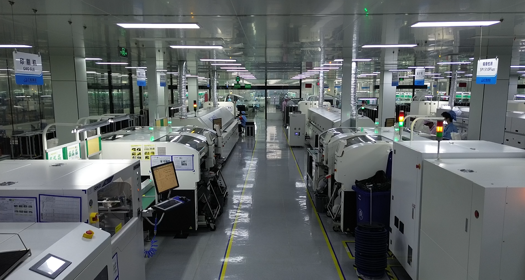
Assembly Considerations
While separate from fabrication, PCB design impacts assembly processes. Solder paste stencil thickness (typically 100-150μm) correlates with pad sizes. Component keep-out zones prevent interference with test points or connectors. Panel fiducials assist pick-and-place machine alignment. Thermal relief patterns balance soldering heat distribution with electrical conductivity.